Question
Question: When a p-n junction is reverse biased A.) Electrons and holes are attracted towards each other and...
When a p-n junction is reverse biased
A.) Electrons and holes are attracted towards each other and move towards the depletion region.
B.) Electrons and holes move away from the junction depletion region.
C.) Height of the potential barrier decreases.
D.) No change in the current takes place.
Solution
Hint : A p-n junction is said to be in reverse bias if the p-side of the junction is connected to a negative terminal of a battery and the n side is connected to the negative side of the battery. Since the majority carriers in the p side are holes, they will be attracted towards the negative terminal which is attached to the p side, and the electrons in the n-side will also be attracted towards the positive terminal which is connected to it.
Complete step by step answer:
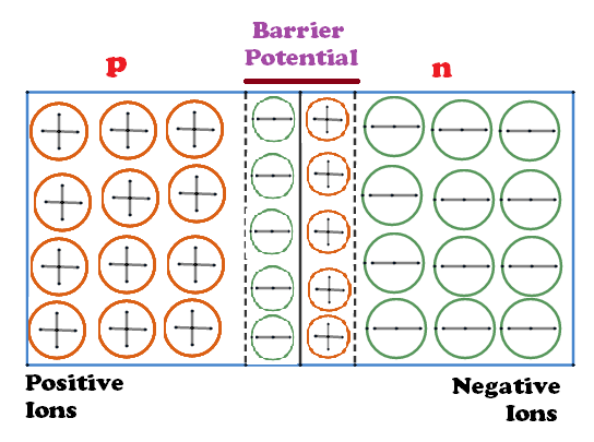
A diagram for the p-n junction is given below,
Semiconductors are materials whose conductivity lies between the conductivity of metals and the conductivity of insulators. There are mainly two types of semiconductors,
Intrinsic Semiconductors- These are pure semiconductors with no amount of doping present in them. ex- Silicon, Germanium
(i)Extrinsic Semiconductors- These are semiconductors which are doped with trivalent or pentavalent atoms to improve the electrical conductivity of a semiconductor.
The extrinsic semiconductors are of two kinds,
P-type semiconductor- When a pure semiconductor like Silicon or Germanium is doped with trivalent impurities like Boron or Aluminium, we get a p-type semiconductor.
N-type semiconductor- When a pure semiconductor like silicon or germanium is doped with pentavalent impurities like Arsenic or Phosphorus, we get an n-type semiconductor.
When a p-type semiconductor and an n-type semiconductor forms an interface or boundary a p-n junction is formed.
When a p-n junction is formed there will be a barrier potential formed due to the minority charge carriers in the p side and the n side.
These minority carriers were once part of the p or n side. When the junction was formed, these charge carriers diffused from the n side or p side to the opposite side.
The diffusion went on till the majority charge carriers which were diffused, set up an electric field across the junction due to charge difference across the junction, that would eventually counteract the diffusion process and stop it.
This electric field is known as the barrier potential. This potential prevents movement of majority carriers.
So holes (majority carriers in p side) cannot go to n side, and electrons (majority carriers in n-side) cannot go to p-side. So the current due to the majority carriers is zero in this position.
So, when the junction is reverse biased that is when the p side is connected to the negative terminal, and the n side is connected to the positive terminal of the battery, the electrons in the n side will be attracted towards the positive terminal, and the holes in the p side will be attracted towards the negative terminal. So, the charged particles will move away from the depletion region.
Such a motion of charged particles increases the width of the depletion layer, which causes a higher impedance path across the junction. There is a chance of a leakage current across the junction, but the current is very small in magnitude usually in the microampere range.
So, the answer to the question is the option (B)
Note : The p-n junction is the basic building block for many electronic devices like diodes, transistors, FET's etc..
The barrier potential for a silicon diode is 0.3V while the barrier potential for a germanium diode is 0.7V.
When an external potential is applied to the p-n junction, the barrier reduces until it becomes zero when the external voltage is greater than the barrier potential.
When the reverse bias voltage is kept on increasing, the p-n junction will breakdown and allow a large amount of current to pass through it. The reverse bias voltage in which the breakdown of the junction occurs is known as the breakdown voltage.