Question
Question: Two following figures show a logic gate circuit with two inputs A and B and the output Y. The voltag...
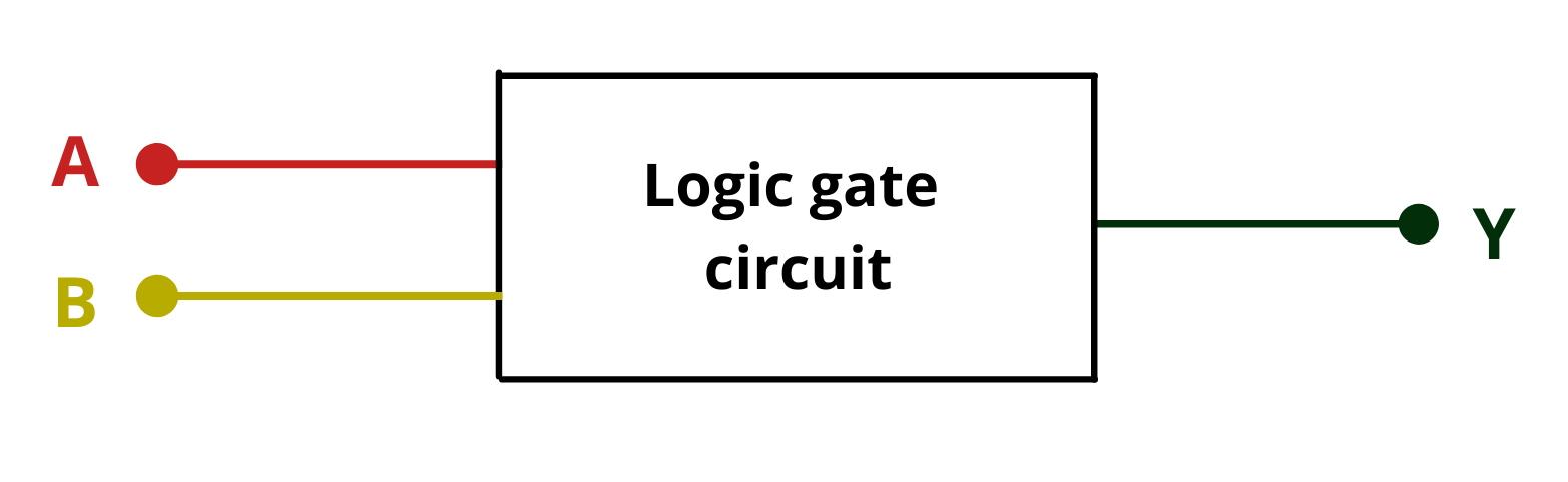
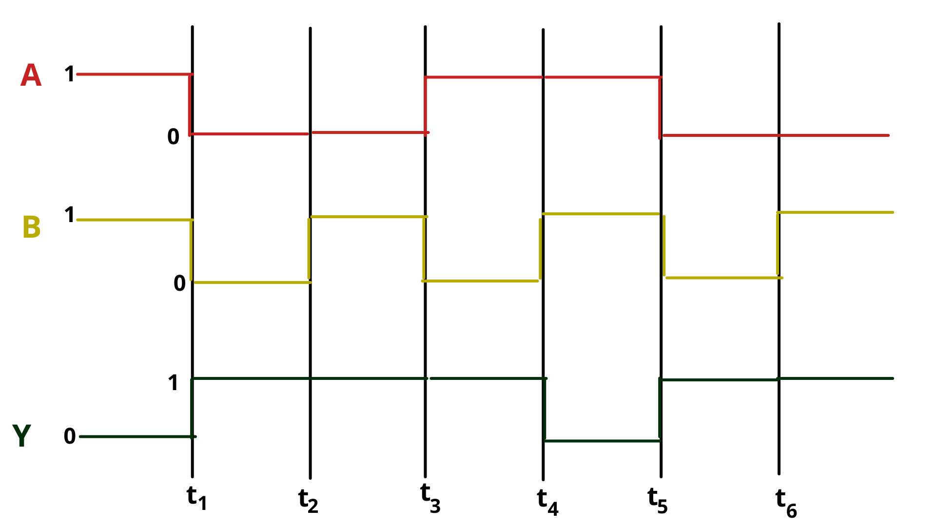
Two following figures show a logic gate circuit with two inputs A and B and the output Y. The voltage waveforms of A, B and Y are as given.
The logic gate is
A. NOR gate
B. OR gate
C. AND gate
D. NAND gate
Solution
In this problem two inputs are given and one output is given in the form of a voltage wave. Based on the input and output values we need to find the logic gate circuit. Draw the truth table for the given six intervals and compare it with the truth tables of NOR gate, OR gate, AND gate and NAND gate.
Complete step by step answer:
Let us draw the truth table for the given circuit. At time interval t1 the input is (1,1) and the output is Y=0. Similarly, at time interval t2 the input is (0,0) and the output is Y=1.
At t3 input is (0,1) and the output is Y=1
At t4 input is (1,0) and the output is Y=1
At t5 input is (1,1) and output is Y=0.
Using this information, the truth table will be as follows:
| A | B | Y |
|---|---|---|
| 1 | 1 | 0 |
| 0 | 0 | 1 |
| 0 | 1 | 1 |
| 1 | 0 | 1 |
| 1 | 1 | 0 |
The truth tables for NOR, OR, AND and NAND gates are given below:
Truth table for NOR gate:
| Input A | Input B | Output |
|---|---|---|
| 0 | 0 | 1 |
| 0 | 1 | 0 |
| 1 | 0 | 0 |
| 1 | 1 | 0 |
Truth table for OR gate:
| Input A | Input B | Output |
|---|---|---|
| 0 | 0 | 0 |
| 0 | 1 | 1 |
| 1 | 0 | 1 |
| 1 | 1 | 1 |
Truth table for AND gate:
| Input A | Input B | Output |
|---|---|---|
| 0 | 0 | 0 |
| 0 | 1 | 0 |
| 1 | 0 | 0 |
| 1 | 1 | 1 |
Truth table for NAND gate:
| Input A | Input B | Output |
|---|---|---|
| 0 | 0 | 1 |
| 0 | 1 | 1 |
| 1 | 0 | 1 |
| 1 | 1 | 0 |
The truth table for the given logical gate circuit is the same as the truth table for NAND gate. Therefore, the logic gate is a NAND gate.
So, the correct answer is Option (D).
Note: NAND gate is a combination of AND gate and NOT gate. In AND gate the output is 1 when the at least one input is 0 as the output for 0 input will be zero and NOT for zero is 1 .NAND gate forms the basis of most practical gates. For NAND gate the output is 0 when both the inputs are 1.