Question
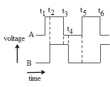
Question: The waveforms A and B given below are given as input to a NAND gate. Then, its logic output is y is ...
The waveforms A and B given below are given as input to a NAND gate. Then, its logic output is y is
A.)For t1 to t2; y=0
B.)For t2 to t3; y=1
C.)For t3 to t4; y=1
D.)For t4 to t5; y=0
E.)For t5 to t6; y=0
Solution
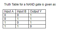
Hint: NAND gate is the combination of a NOT gate and a AND gate. The property of AND is that its output is equal to the product of the input while the NOT gate gives output opposite to the input fed to it.
Detailed step by step answer:
A NAND gate is made by connecting a NOT gate and a AND gate with each other. The symbol for NAND gate is given as
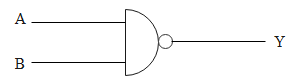
The Boolean expression for a NAND gate is given as
Y = \mathop {A.B}\limits^{\\_\\_\\_\\_\\_\\_} = \mathop A\limits^{\\_\\_} + \mathop B\limits^{\\_\\_}
For t1 to t2; we have A = 1 and B = 0, using the Boolean algebra or the truth table for NAND gate we get y = 1
For t2 to t3; we have A = 1 and B = 1, using the Boolean algebra or the truth table for NAND gate we get y = 0
For t3 to t4; we have A = 0 and B = 1, using the Boolean algebra or the truth table for NAND gate we get y = 1
For t4 to t5; we have A = 0 and B = 0, using the Boolean algebra or the truth table for NAND gate we get y = 1
For t5 to t6; we have A = 1 and B = 0, using the Boolean algebra or the truth table for NAND gate we get y = 1
On the basis of the above results, the correct option is C from the given choices.
Note:
1. In digital electronics, the higher value of voltage is considered 1 whereas lower value of voltage is considered 0.
2. In order to obtain a NAND gate, the AND and NOT gate must be connected in series with each other. Attaching them in parallel will not give the desired gate.