Question
Question: The output (X) of the logic circuit shown in diagram will be given as,  of the logic circuit shown in diagram will be given as,
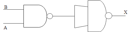
A.X=A⋅BB.X=A⋅BC.X=A⋅BD.X=A+B
Solution
A NAND gate also known as not-and gate is a logic gate which creates an output which is incorrect only if all its inputs are true. A NOT gate is otherwise known as an inverter. It is a logic gate which represents the logical negation. An electronic circuit device that creates an inverted version of the input as the output is known as NOT gate. This all will help you in answering this question.
Complete step by step answer:
A NAND gate is derived from an AND gate. It acts complimentary to the AND gate. The outputs of NAND gates will be high when any of the inputs are made low. The symbol of NAND gate is an AND gate itself with a small circle on the output. The small circle indicates the inversion. A NOT gate acts as logical negation on the input. It means that if the input is true, then the output will be false. In the same sense, a false input will be given as a true output.
Here in the question the first gate given is NAND gate and the second gate given is a NOT gate. Therefore the combination will result in a AND gate. The output of a AND gate is given as,
X=A⋅B
So, the correct answer is “Option C”.
Note: NAND gates can be useful in producing any other kind of logic gate functions and in general the NAND gate will be forming the basis of most practical logic circuits. A gate is defined to be sinking current if it gives a path for current in between the ground and the output terminal.