Question
Question: The n-side of the depletion layer of a p-n junction. \[A.\] Always has the same width as the p-sid...
The n-side of the depletion layer of a p-n junction.
A. Always has the same width as the p-side.
B. Has no bound charges
C. Is negatively charged.
D. Is positively charged.
Solution
Hint : We will look at the components of p−side and n−side of a p-n junction diode and also about the minority charge carriers. The depletion region is formed by the majority charge carried of the particular side. We can then see the charge at the depletion layer of a particular side.
Complete solution: First of all let us understand the majority and minority charge carriers in N−type and P−type semiconductors. In N−type they have excess free electrons compared toP−typewhich have excess holes. So, the minority carriers in both will be holes and electrons respectively.
Now, if we look at how a depletion layer is formed in p-n junction diodes which are formed by combining an N−type and a P−type semiconductor, electrons and holes diffuse into regions with lower concentration. Therefore, free electrons from n−side diffuse into p−side and holes from p−side diffuses into n−side.
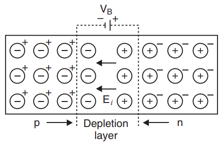
Now, at the n−side region near the junction, the free electrons are gone by the diffusion of electrons to p−side and recombination of electrons to holes that are diffused fromp−side. Similarly, the holes from p−side will also be gone. As a result, majority charge carriers are depleted at the junction which is called a depletion layer.
Due to this depletion layer, both the sides will be charged as, n−side will be positively charged and p−side will be negatively charged. Therefore, option d is the correct answer.
Note: We must be aware of the fact that the charges at the depletion layer are non-mobile charges and they act like a barrier that opposes the flow of electrons and holes. The width of this layer will change according to the biasing conditions and hence the potential difference will change. That means the charge at either side will differ.