Question
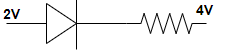
Question: The forward biased diode connection is: (A) 
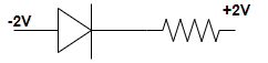
(B)
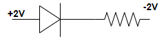
(C)
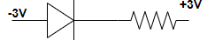
(D)
Solution
This question can be solved by having an understanding of a semiconductor device that is known as p-n junction or junction diode. These kinds of devices are made of semiconductor materials having the energy band gap of <3eV between conduction band and valence band.
Complete step by step answer:
Step 1: A p-n junction or junction diode is said to be in forward bias if the positive terminal of the external battery B is connected to the p-side and the negative terminal is connected to the n-side of p-n junction.
The majority carriers, electrons in the n-region are repelled by the negative potential due to battery B and move towards the p-n junction. Similarly, the majority carriers, holes in the p-region are repelled by the positive potential due to battery B, towards the junction.
The positive potential of p-region attracts the electrons from the n-region and negative potential of n-region attracts the holes from the p-region.
Step 2: As shown in this question from all the given options, option (C) is in forward bias in which the p-side of the diode is connected to the +2V of the battery and n-side of the diode is connected to the -2V of the battery.
As we know that majority carriers, holes in the p-region will be repelled and majority carriers, electrons in the n-region will be repelled. Due to this, the diffusion of majority carriers takes place across the junction.

So, this given configuration is in forward bias i.e. the option (C) is correct.
Note: It should always be remembered that at zero kelvin temperature, electrons are not able to cross even the given energy band gap and hence the conduction band remains totally empty. Therefore, the semiconductor at zero kelvin behaves as an insulator.