Question
Question: Identify the logic operation carried out by the following circuit. 
(A) AND
(B) NAND
(C) NOR
(D) OR
Solution
To solve this problem,we are going to apply the concept of logic gate and we know that all logic gates used here are NAND gates. We should know Boolean algebra for NAND gates.
Complete step by step answer:
Logic gates Logic gates are the basic building blocks of any digital system. It is an electronic circuit having one or more than one input and only one output. The relationship between the input and the output is based on certain logic. Based on this, logic gates are named as AND gate, OR gate, NOT gate etc.
Most logic gates have two inputs and one output and are based on Boolean algebra. At any given moment, every terminal is in one of the two binary conditions false (high)(1) ortrue(low)(0). False represents 0, and true represents 1. Depending on the type of logic gate being used and the combination of inputs, the binary output will differ. There are 7 basic types of gates and all others are constructed from these basic gates.
NAND| 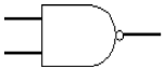 |
|
---|---|---
In question Terminal A is connected to an NAND gate and Terminal B with another NAND gate. The output of both NAND gates is again connected to NAND gate.
The NAND gate operates as an AND gate followed by a NOT gate. It acts in the manner of the logical operation followed by negation. The output is if both inputs are Otherwise, the output is
| Terminal A | Terminal B | Output of Terminal A | Output of Terminal B | Output of 3rd NAND Gate |
|---|---|---|---|---|
| 1 | 1 | 0 | 0 | 1 |
| 1 | 0 | 0 | 1 | 1 |
| 0 | 1 | 1 | 0 | 1 |
| 0 | 0 | 1 | 1 | 0 |
So, the summarized Boolean table is,
| Terminal A | Terminal B | Output |
|---|---|---|
| 1 | 1 | 1 |
| 1 | 0 | 1 |
| 0 | 1 | 1 |
| 0 | 0 | 0 |
This Boolean table resembles the table for OR gate.
So the logic operation carried out by the given circuit isOR
Note: Sometimes students get confused in between AND and NAND gates because the symbol of both of them are nearly similar except for the NAND gate which contains a small circle like structure before the final out of it. This small circle-like structure is NOT gate which makes the output of the AND gate different from the NAND gate.