Question
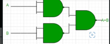
Question: The given circuit diagram shows the implementation of a logic function using NAND gates....
The given circuit diagram shows the implementation of a logic function using NAND gates.
Answer
The circuit represents an OR gate.
Explanation
Solution
The circuit consists of three NAND gates. The first two NAND gates have their inputs tied together, making them function as NOT gates, producing A and B respectively. These inverted outputs are then fed into a third NAND gate. The output of this third NAND gate is A⋅B. By applying De Morgan's theorem (X⋅Y=X+Y) and the double negation rule (X=X), the expression simplifies to A+B, which is the Boolean expression for an OR gate.