Question
Question: Draw the typical input and output characteristics of a \(n - p - n\) transistor in \(CE\) configurat...
Draw the typical input and output characteristics of a n−p−n transistor in CE configuration. Show how these characteristics can be used to determine
(a) the input resistance ( ri ) and
(b) current amplification factor (β) .
Solution
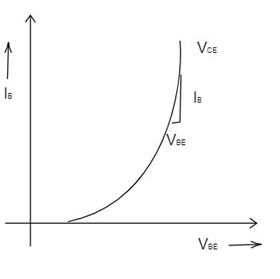
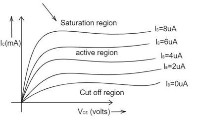
The n−p−n transistor has the input, output and the transfer characteristics. Draw the input characteristics between base current and base emitter voltage and the output characteristics between the collector current and the common emitter voltage.
Complete step by step solution:
(a) The input resistance is also known as input impedance. It is defined as the ratio of the changes in the base emitter voltage to the corresponding change in the base current at a given particular common emitter voltage in the transistor.
The formula of the input impedance is given by
ri=ΔIBΔVBE ( at a given VCE )
(b) The term current amplification factor is also known as the current gain. It is obtained by dividing the small change in the collector current to that of the corresponding change in the base current of the transistor at constant common emitter voltage.
The formula of the current amplification factor is given by
β=ΔIBΔIC ( at a given VCE )
The following graph represents the input characteristics of the n−p−n transistor. It shows that to a certain point, when the base current increases the base emitter voltage remains the same.
The following graph shows the output characteristics of the n−p−n transistor. It includes the cut off, active and the saturated regions of the base current where the common emitter voltage is constant.
Note: In the n−p−n transistor, the P - type of the semiconductor is made connected between the N - type of the semiconductor. It is most commonly used and it looks like the PN junction diode connected back to back. In this transistor, the electron transfers from the base to the collector.