Question
Question: Draw the circuit diagram of a full-wave rectifier by the use of two p-n junction diodes and describe...
Draw the circuit diagram of a full-wave rectifier by the use of two p-n junction diodes and describe its working. Represent the input and output waveforms.
Solution
Full-wave rectification is a rectifier, which rectifies the negative component of the input voltage into a positive voltage, then converts it into pulse current which is a direct current using a diode bridge configuration. This will help you in answering this question.
Complete step-by-step solution
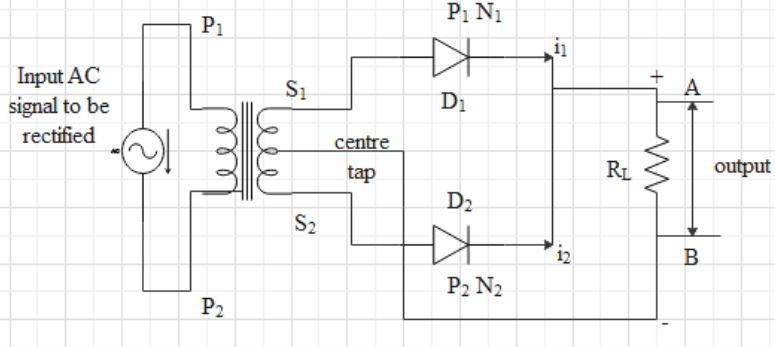
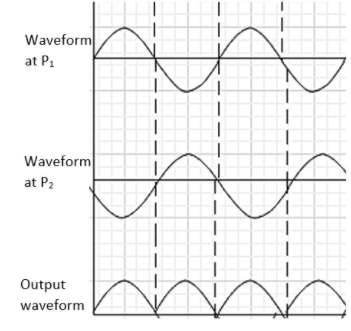
First of all, let us draw the circuit diagram and also let us explain the working. The AC input voltage across the secondary S1 and S2varies the polarity after each half cycle. Let us assume during the first half cycle of the input AC signal, the terminal S1 be the positive relative to center tap O and S2 be the negative relative to O. Then diode D1 will be in forwarding bias and diode D2 will be in reverse biased. Hence the diode D1 conduct while diode D2 will not conduct.
In the next half-cycle, the terminal S1 will be negative with respect to center tap O and S2 is positive relative to O. then diode D2 is forward bias and diode D1 is reverse biased. Therefore diode D2 conduct while diode D1 does not. The direction of current in the load resistance RL will be the same from A to B for both the half cycles. Hence for the input AC signal, the output current will be a continuous series of unidirectional pulses.
Note: The Bridge Rectifier circuits are commonly useful in power supply for different appliances because they are capable of converting the High AC voltage into Low DC voltage. By the way, the half-wave rectification avoids just the negative voltage component with the use of a single diode before changing to DC.