Question
Question: Draw the circuit arrangement for studying V-I characteristics of a P-N junction diode in reverse bia...
Draw the circuit arrangement for studying V-I characteristics of a P-N junction diode in reverse bias. Plot V-I characteristics in this case.
Solution
The P-N junction is reverse biased, that means the positive terminal of a voltage source is connected to the n-type region and the negative terminal of the source is connected to the p-type region. Cathode is at higher voltage than anode.
Complete step by step answer:
A P-N junction is a junction between two semiconductor devices, namely P and N type, inside a semiconductor. The P side is positive, and has an excess number of holes whereas the N type is negative having excess number of electrons.
In reverse biasing, the positive terminal of the battery is connected to N type and the negative terminal of the battery is connected to P type. In came of this biasing current flow is zero, this happens because cathode is made more positive with respect to anode.
The circuit diagram for a PN Junction in reversed bias is as follows:
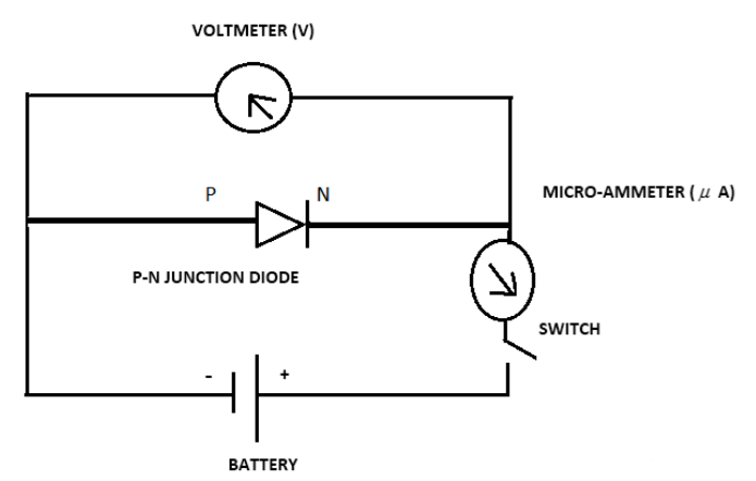
This circuit helps us in obtaining V-I characteristics in reverse bias.
When a P-N junction is reverse biased the negative terminal of the battery attracts the holes in P type towards itself and the positive terminal of the battery attracts the free electrons in N type towards itself. This results in creation of more positive impurity ions in the depletion layer which makes the layer of positive impurity ions thicker.
The V-I characteristics:
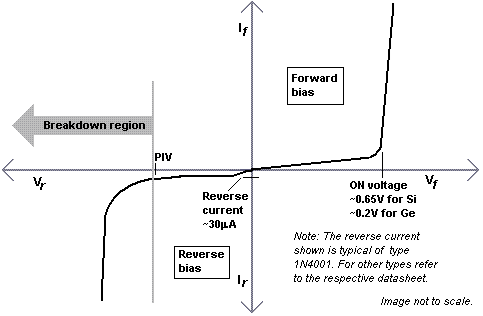
Here, voltage is taken along the X axis, and Current is taken along the Y axis.
In reverse bias, small or approximately no current flows.
Note: The maximum reverse voltage that can be applied to PN Junction is limited by Breakdown. Value of this voltage is referred to as breakdown voltage. In reverse bias, N side is held at a higher voltage than the P side.