Question
Question: Draw a diagram to show how NAND gates can be combined to obtain an OR gate. (Truth table is not requ...
Draw a diagram to show how NAND gates can be combined to obtain an OR gate. (Truth table is not required).
Solution
A NAND gate is a logic gate that consists of two different gates called NOT and AND. A NOT gate allows complements of the value that is fed into the logic gate, it converts 1 to 0 and 0 to 1 . Whereas AND gate is similar to the multiplication or Intersection of operation of two signals. The AND of two similar inputs will give the same output as the input, but for 1 AND 0 it returns 0 .
Complete Answer:
The following diagram shows how three NAND gates can be combined to obtain an OR gate-
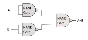
In the figure, the first two NAND gates are connected individually to both signals A and B . The purpose of this gate is to complement the values of both A and B . It acts as a NOT gate.
So if A is 1 the output of the gate will be 0 , and if A is 0 then the output of the gate will be 1 .
Same goes for B .
Now another NAND gate combines the output made by the previous gates. At this gate, the complements of both A and B go through these two processes-
AND- The output coming from the first two NAND gates first goes through the AND process.
NOT- Now again the results obtained after this “AND” operation is complemented back with this NOT part of the gate.
The results thus obtained are similar to the result that would have been observed if an OR gate was used.
Note:
When the same signal is fed into both inputs of any gate, the set of inputs reduces from four to only two where both of these responses are either 1 or 0 . This is what happens in the solution of this problem when the input signals A and B go through their first NAND gates.