Question
Question: Draw a circuit diagram of a transistor amplifier in CE configuration. Define the terms: (i) Inpu...
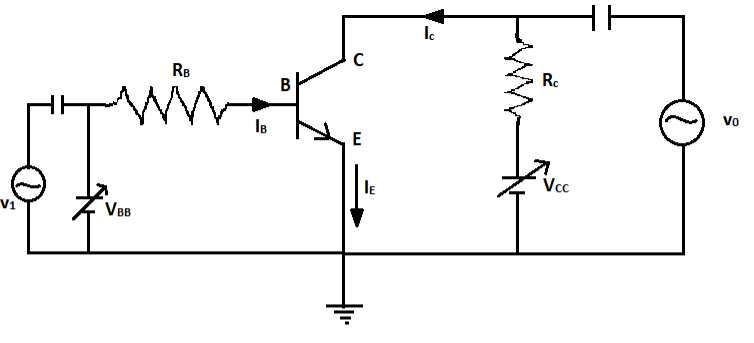
Draw a circuit diagram of a transistor amplifier in CE configuration.
Define the terms:
(i) Input resistance and
(ii) Current amplification factor.
How are these determined using typical input and output characteristics?
Solution
Recall the common emitter configuration of a transistor amplifier. Also recall its circuit diagram, its V-I characteristics graph. Always remember, in common emitter configuration, the input current and the output voltage are taken as the independent variables, whereas the input voltage and output current are the dependent variables.
Complete step by step solution:
The circuit diagram of a transistor amplifier in Common-Emitter configuration is given by,
(i) Input resistance :- It is defined as the ratio of change in base-emitter voltage to the change in base current at constant VCE . The change in base-emitter voltage that is ΔVBE and the change in base current that is ΔIB can be calculated from the input characteristics of the transistor amplifier in CE configuration.
Mathematically, Input resistance is defined by,
RiB=(ΔIBΔVBE) at constant VCE
Where, ΔVBE is the change in base-emitter voltage
ΔIB is the change in the base current
VCE is the collector-emitter voltage
For finding the input resistance, we have to mark a point P on the input characteristics and then draw a tangent at point P and then the reciprocal of slope AB will give us the input resistance.
(ii) Current amplification factor :- It is defined as the ratio of the change in collector current to the change in the base current taking collector voltage constant. It is denoted by β
Mathematically, current amplification factor is defined by,
β=(ΔIBΔIC) at constant VCB.
Where, ΔIC is the change in collector current.
ΔIB is the change in the base current.
The value of current amplification factor is obtained from the Output characteristic graph that is IC versus VCE plot by using different values of IB.
Note: The common-emitter configuration provides good current gain and voltage gain. As the input resistance is of very low value, a small value of ΔVBE is enough to produce a large current flow of the base current. The current gain in Common Emitter connection is very high. This is the reason this circuit connection is mostly used in all transistor applications.