Question
Question: Derive the expression for voltage gain of a transistor amplifier in CE configuration terms of the lo...
Derive the expression for voltage gain of a transistor amplifier in CE configuration terms of the load resistance RL, current gain βα and input resistance. Explain why input and output voltages are in opposite phases.
Solution
Here, we will use Kirchhoff’s law to derive the expression for a voltage gain of a transistor amplifier in CE configuration. Also, keep in mind that an amplifier is a device that is used to increase the amplitude of the input signal.
Complete step by step solution:
As we know, the operation of a transistor as an amplifier is possible only if we fix its operating point in the middle of its active region.
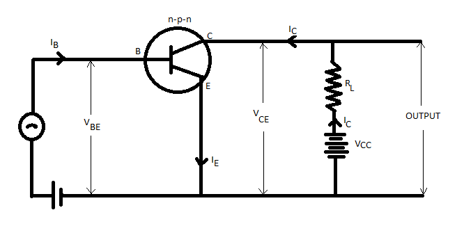
Now, we all know that amplifiers are used to amplify the alternating signals. Therefore, we will superimpose the ac input signal vi on vBB. The output will be taken between the collector and ground.
Now, for an amplifier, we will take vi=0.
Hence, using Kirchhoff’s law to the output loop, we get
VCC=VCE+ICRL
Now, using Kirchhoff’s law to the input loop, we get
VBB=VBE+IBRB
Here, when Vi is not zero, we get
VBB+vi=(VBE+ΔVBE)+(IB+ΔIB)RB
Or VBB+vi=VBE+IBRB+ΔVBE+ΔIBRB
Here, the change in VBE can be related to the input resistance ri and the change in IB is given by
ΔVBE=ΔIBri
So, we will get
VBB+vi=VBE+IBRB+ΔIB(RB+ri)
Now, we will get the value of vi as
VBB+vi−VBB=VBE+IBRB+ΔIB(RB+ri)−VBE−IBRB
⇒vi=ΔIB(RB+ri)
⇒vi=rΔIB
Now, we can say that a change in IB causes a change in IC. Therefore, we define will a new parameter βac which is also similar to βdc, as
βac=ΔIBΔIC=iBiC
This equation is also known as the current gain Ai. Usually, βac remains close to βdc in the linear region of the output characteristics. Now, the change in ICdue to a change in IB leads to the change in VCE and the voltage drop across the resistor RL, because VCC is fixed.
We can see the changes in the equation given below
ΔVCC=ΔVCE+RLΔIC
Here, if we consider ΔVCC=0,
∴ΔVCE=−RLΔIC
Now, we know βac=ΔIBΔIC
Therefore, value of ΔICfrom this equation to the above equation, we get
v0=ΔVCE=−βacRLΔIB
Therefore the voltage in the amplifier is given by
Av=viv0
⇒Av=rΔIBΔVCE
⇒Av=r−βacRL
Here, the negative sign shows that the output voltage is in the opposite phase to the input voltage.
Note: Consider that we apply an input signal voltage Vi to the emitter-base circuit. We will observe that there will be a change in base current and collector current respectively.
Also, when the input voltage increases, the current through the base-circuit also increases. This will lead to a fall in the voltage between the collector and emitter terminals.