Question
Question: A transistor is used in common-emitter mode in an amplifier circuit. When a signal of \(20mV\) is ad...
A transistor is used in common-emitter mode in an amplifier circuit. When a signal of 20mV is added to the base-emitter voltage, the base current changes by 20μA and the collector current changes by 2mA. The load resistance is 5kΩ. Calculate (a) the factor β, (b) the input resistance RBE, (c) the trans conductance and (d) the voltage gain.
Solution
Emitter current for a common emitter configuration is defined as IE=IC+IB, and the current gain is the ratio of IC and IB.
Use Kirchoff’s voltage law to obtain expression for required quantity.
In a transistor, current gain is defined as the factor by which current is amplified in the circuit. Current gain is denoted by β.
The trans conductance of a CE configured transistor is defined as ratio of collector current to the base emitter input voltage.
Voltage gain is defined as the factor by which input voltage is amplified.
Formula used:
β=ΔIBΔIC
Complete step-by-step answer:
In the Common Emitter configuration, the input signal is applied between the base and the emitter, and the output is taken from between the collector and the emitter as shown. Common emitter type of configuration is the most commonly used for transistor based amplifiers.
In common emitter configuration of bipolar junction transistor, the current flowing out of the transistor must be equal to the currents flowing into the transistor as the emitter current is given as
IE=IC+IB
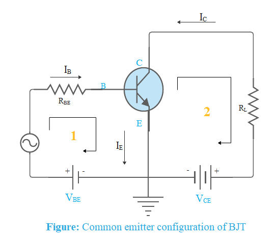
Load resistance RL is connected in series with the collector. The current gain of the common emitter transistor configuration is written as
β=IBIC
In this question, IC is 2mA and IB=20μA
Therefore, β=20μ2m=20×10−62×10−3=100
Applying Kirchoff’s law in loop 1, we get
−VBE+IBRBE=0
⇒RBE=IBVBE=20μA20mV=103Ω
RBE=1kΩ
Trans conductance of a CE amplifier is the ratio of current gain to the voltage applied. Therefore,
Trans conductance = VBEIC=20mV2mA=0.1mho
The change in output voltage can be calculated by applying Kirchoff’s voltage law in loop 2
−VCE+ICRL=0
⇒VCE=ICRL=2mA×5kΩ=10V
Applied signal voltage is, Vin=20mV
Voltage gain = VinVout=VBEVCE=20mV10V=500
Note: Common emitter configuration of bipolar junction transistor has a greater input impedance, current and power gain than that of the common base configuration but its voltage gain is much lower. The common emitter configuration acts as an inverting amplifier circuit. This implies that the resulting output signal has a 180∘ phase-shift with regards to the input voltage signal.