Question
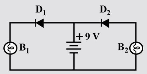
Question: (a) In the following diagram, which bulb out of \[{B_1}\] and \({B_2}\) will glow and why?  In the following diagram, which bulb out of B1 and B2 will glow and why?
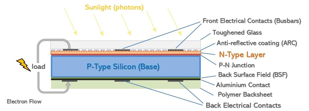
(b) Draw a diagram of an illuminated p-n junction solar cell.
(c) Explain briefly the three processes due to which generation of emf takes place in a solar cell.
Solution
Hint(a) Current always flows in forward biasing condition and doesn’t flow in reverse biasing condition. So, identify the biasing of the diodes.
(b) A solar cell is basically a junction diode, although its construction is a little bit different from conventional p-n junction diodes. A very thin layer of p-type semiconductor is grown on a relatively thicker n-type semiconductor. We then apply a few finer electrodes on the top of the p-type semiconductor layer.
(c) The three processes due to which generation of emf takes place in a solar cell are
(i) Generation of electron-hole pairs due to light close to the junction.
(ii) Separation of electrons and holes due to the electric field of the depletion region. Electrons are swept to n-side and holes to p-sides.
(iii) The electrons reaching the n-side are collected by the front contact and holes reaching p-side are collected by the back contact.
Complete step-by-step solution :
(a) As from the diagram it is clear that current has to flow through the diode for the glowing of the bulb because Current always flows in forward biasing condition and doesn’t flow in reverse biasing condition. So, we first identify the biasing of the diodes.
In the diagram, diode D1, having its p side connected with the positive terminal of the battery, is in forward bias and diode D2, having its n side connected with the positive terminal of the battery, is in reverse bias. So current will flow through D1 and D2 will not allow flowing the current.
Hence, bulb B1 will glow and bulb B2 will not glow.
(b) A solar cell is basically a junction diode, although its construction is a little bit different from conventional p-n junction diodes. A very thin layer of p-type semiconductor is grown on a relatively thicker n-type semiconductor. We then apply a few finer electrodes on the top of the p-type semiconductor layer.
Here is the diagram of an illuminated solar cell:
(c) Three processes due to which generation of emf takes place in a solar cell are:
(i) Generation of electron-hole pairs due to light close to the junction.
(ii) Separation of electrons and holes due to the electric field of the depletion region. Electrons are swept to n-side and holes to p-sides.
(iii) The electrons reaching the n-side are collected by the front contact and holes reaching p-side are collected by the back contact. Thus p-side becomes positive and n-side becomes negative giving rise to photo voltage.
Note: During formation of p-n junction p-side has excess holes and n-side has excess electrons. Hence, current tends to flow due to diffusion from p-side to n-side. This does not happen without an external bias because of the potential barrier at the junction.
When the p-side is given a potential higher than the n-side, it aids in the flow of this diffusion current and hence, current flows.
Advantages of Solar Cell:
1. No pollution associated with it.
2. It must last for a long time.
3. No maintenance cost.