Question
Question: A full wave rectifier circuit with diodes ($D_1$) and ($D_2$) is shown in the figure. If input suppl...
A full wave rectifier circuit with diodes (D1) and (D2) is shown in the figure. If input supply voltage Vin = 220sin (100 π t) volt, then at t = 15 msec
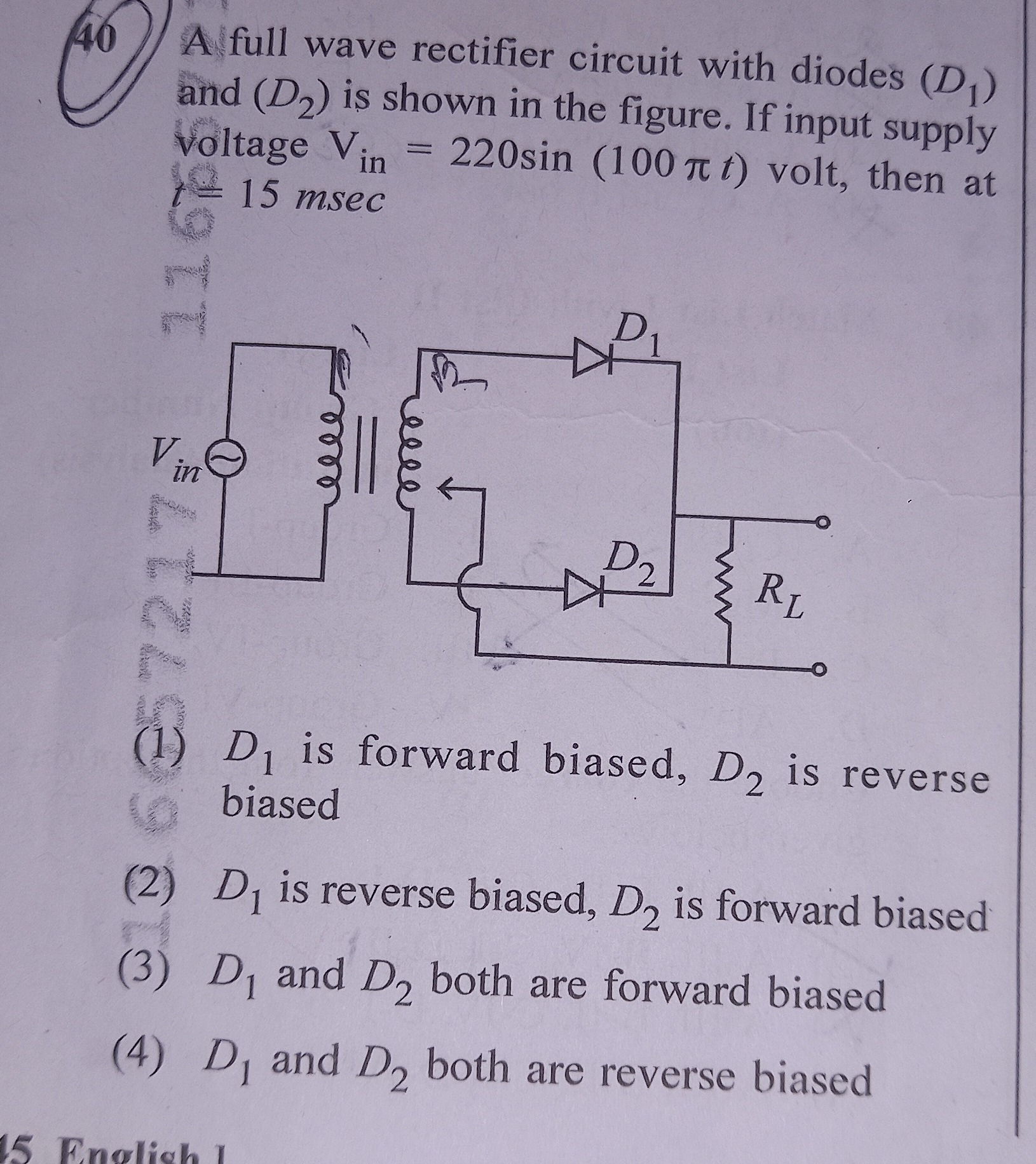
D1 is forward biased, D2 is reverse biased
D1 is reverse biased, D2 is forward biased
D1 and D2 both are forward biased
D1 and D2 both are reverse biased
(2) D1 is reverse biased, D2 is forward biased
Solution
To determine the biasing state of the diodes D1 and D2 at t=15 msec, we need to analyze the input voltage at that specific time.
-
Analyze the input supply voltage: The input supply voltage is given by Vin=220sin(100πt) volt. We need to find the sign of Vin at t=15 msec.
-
Calculate the phase angle at t=15 msec: Substitute t=15 msec=15×10−3 s into the argument of the sine function: Phase angle θ=100πt=100π(15×10−3)=1.5π radians.
-
Determine the sign of Vin: Now, evaluate sin(θ)=sin(1.5π)=sin(270∘)=−1. Therefore, Vin=220×(−1)=−220 volt.
-
Analyze the transformer and secondary coil polarity: Since Vin is negative at t=15 msec, it implies that the top terminal of the primary winding is negative with respect to the bottom terminal. Assuming a standard transformer winding (dots on the same side), the phase relationship dictates that:
- The top end of the secondary coil (connected to the anode of D1) will be negative with respect to the center tap.
- The bottom end of the secondary coil (connected to the anode of D2) will be positive with respect to the center tap.
Let the center tap be at 0 V (ground).
- Potential at the anode of D1 is negative (e.g., −Vs, where Vs is the peak voltage across half the secondary winding).
- Potential at the anode of D2 is positive (e.g., +Vs).
- The cathodes of both D1 and D2 are connected to the load resistor RL, which is connected to the center tap. The output voltage across RL is always positive (or zero) in a full-wave rectifier. So, the common cathode point will be at a positive potential (or zero) relative to the center tap.
-
Determine the biasing of diodes D1 and D2:
-
Diode D1:
- Anode is at a negative potential.
- Cathode is at a positive (or zero) potential (output voltage).
- Since the anode potential is less than the cathode potential (VA<VK), diode D1 is reverse biased.
-
Diode D2:
- Anode is at a positive potential.
- Cathode is at a positive (or zero) potential (output voltage).
- Since the anode potential is greater than the cathode potential (VA>VK), diode D2 is forward biased.
-
Therefore, at t=15 msec, D1 is reverse biased and D2 is forward biased.