Question
Question: A common emitter amplifier is designed with a n-p-n transistor.(\(\alpha =0.99\)). The input impedan...
A common emitter amplifier is designed with a n-p-n transistor.(α=0.99). The input impedance is 1kΩ and load is 10kΩ. The voltage gain will be:
a) 9900
b) 99
c) 9.9
d) 990
Solution
In the above question a n-p-n transistor is used as a common emitter amplifier. Hence the voltage gain when connected across a a.c. is given by Voltage gain(AV) = current gain(β) !!×!! resistance gain(AR)....(1).In the question the current gain of common base configuration is given to us, hence we can use the relation between !!α!! and β and then substitute for β in the above equation to get the voltage gain in common emitter amplifier.
Complete answer:
To begin with let us first define the voltage gain, current gain and the resistance gain in a n-p-n transistor using a circuit diagram for common emitter amplifiers.
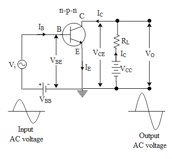
The voltage gain for a n-p-n transistor is defined as the small change in the output voltage(ΔVCE) to a small change in the input voltage (ΔVBE) i.e. AV=ΔVBEΔVCE.
The current gain in an common emitter configuration is defined as the ratio of small change in collector current(ΔIC) to small change in base current (ΔIB) i.e. β=ΔIBΔIC
Resistance gain is defined as the ratio of Load resistance (RL )to the impedance(RI ) in an Ac circuit.
In the current gain for common base configuration is given to us i.e. α=0.99. The relation between the current gain β and α is given by,
β=1−αα. Hence β from the adjacent equation is numerically equal to,
β=1−ααβ=1−0.990.99=0.010.99=99
The resistance gain in the above circuit is numerically equal to,
RGAIN=RIRL=1×10³Ω10×103Ω=10 . Hence substituting the current gain and the resistance gain in equation 1 we get,
!!×!! resistance gain(AR) Voltage gain(AV) = current gain(β) Voltage gain(AV)=99×10=990
So, the correct answer is “Option D”.
Note:
The voltage gain is the ratio of the same physical quantity. Hence the quantity is dimensionless. It is also to be noted that the input and the output voltages are out of phase by an angle of 180 degrees. The basic aim of such transistor amplifiers is to increase the amplitude of the input voltages.